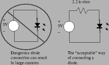
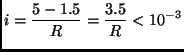
This section discusses methods for driving resistive and capacitive loads from the MicroStamp11's output pins. Some care must be taken in interfacing such loads to an output pin in order to prevent damaging the MicroStamp11. To see how such damage might occur, let's consider consider the circuit shown below in figure 17.
The output pin of the MicroStamp11 can be modelled as an
independent 5 volt voltage source when the pin's logical
state is "high". So let's see what happens if we use the
left hand circuit in figure 17. This
circuit directly connects the output pin to ground through
a light emitting diode (LED). Because of the diode's
orientation, this diode is forward biased. A forward
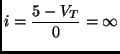
biased diode will drop ![]() volts (
volts (![]() is the diode's threshold voltage
and it lies somewhere between .7 to 1.6 volts depending on
the type of semiconductor material used in the diode).
But the forward biased device is, essentially, a short
circuit which means its resistance is essentially zero.
By Ohm's law, the current,
is the diode's threshold voltage
and it lies somewhere between .7 to 1.6 volts depending on
the type of semiconductor material used in the diode).
But the forward biased device is, essentially, a short
circuit which means its resistance is essentially zero.
By Ohm's law, the current, ![]() , passing through
the diode will be given by the equation
, passing through
the diode will be given by the equation
 |
A circuit that limits the current demand is shown in the
right hand circuit in figure 17.
Since the resistor, ![]() , is in series with the diode, the
current passing through the diode will be limited by the
resistor. The current drawn by this circuit will be given
by the formula
, is in series with the diode, the
current passing through the diode will be limited by the
resistor. The current drawn by this circuit will be given
by the formula
 |
 |
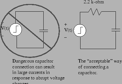
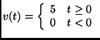
A similar problem will be encountered if we attempt to use
the MicroStamp11 to drive a capacitor. The left hand circuit in figure
18 shows the output pin connected to
ground through a capacitor, ![]() . Now we know that the
current,
. Now we know that the
current, ![]() passing through a capacitor satisfies the
relation
passing through a capacitor satisfies the
relation
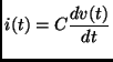 |
 |
Once again,we need to use a resistor in series with the
capacitor to limit the voltage through the capacitor.
This "safer" circuit is shown in the right hand circuit in
figure 18. The size of the current
limiting resistor, ![]() is again determined by Ohm's law.
Note that in response to an abrupt voltage change, the
capacitor appears to be a short circuit. So the required
resistance can be obtained from the equation
is again determined by Ohm's law.
Note that in response to an abrupt voltage change, the
capacitor appears to be a short circuit. So the required
resistance can be obtained from the equation
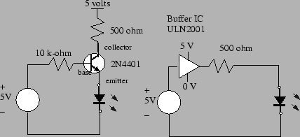
The preceding discussion has shown how we can use current-limiting resistor to restrict the current drawn out of the MicroStamp11 below a specified safe level. In general, however, we should realize that these current levels are very small and in certain cases, they may not be sufficiently large to adequately drive the load. As an example, we can consider the LED circuit shown in figure 17. The brightness of the LED is proportional to current flowing through it. To achieve an adequate brightness level, we may want to drive these LED's at 10 mA, rather than 1 mA.
We can drive our LED's with higher current, provided we
introduce a buffer between the LED and the MicroStamp11.
Two such circuits are shown below in figure
19. The left hand circuit uses an npn
bipolar transistor as a current driver for the LED. A
transistor is a 3-terminal semiconductor device that can
act as an amplifier or an electronic switch.
The three terminals are called the base, collector, and emitter. The labeling of these
terminals is shown in figure 19. The
circuit in figure 19 uses the transistor
as a switch. The output pin is connected to the base
terminal of the transistor through a 10 k-ohm current
limiting resistor. When the output pin goes high (5
volts), then the transistor is switched off and the
collector to emitter path can be treated as an open
circuit. When the output pin goes low (0 volts), then the
transistor is switched on and current flows
through the LED. The virtue of this circuit is that the
current driving the LED is drawn directly from the power
supply through the collector-emitter path, rather than the
base-emitter path. So the current drawn from the
MicroStamp11 is small and we can dramatically reduce the
resistance ![]() to increase the current flowing through the
LED and hence increase its brightness. Note that this LED
driver is actually an inverter for setting the input high
turns off the LED.
to increase the current flowing through the
LED and hence increase its brightness. Note that this LED
driver is actually an inverter for setting the input high
turns off the LED.
Another type of LED driver is shown in the right hand circuit of figure 19. This circuit uses an integrated circuit known as a Darlington current driver (ULN2001) to drive the LED. It is, essentially, the same as the left hand circuit with the exception that we've replaced the single npn transistor by an integrated circuit that can provide a much much larger current than could have been sourced by the single transistor. The other difference is that the ULN2001 does not act as an inverter to the LED is turned on when we set the input line high.